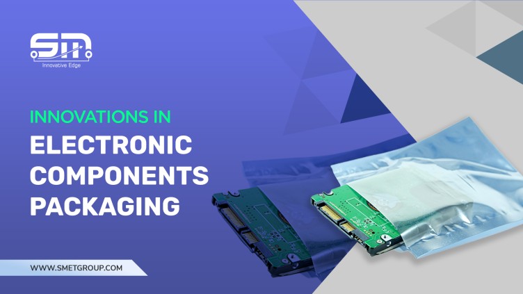
Innovations in electronic packaging focus on improving miniaturization, thermal management, and environmental sustainability. Innovations in electronic components packaging can greatly impact product performance, reliability, and user experience.
In this blog post, we will explore top innovations in electronic component packaging.
1. Miniaturization:
One of the most notable trends in electronic component packaging is miniaturization. One such innovation is Chip-scale Packaging (CSP), which enables the creation of ultra-compact components that are almost the same size as the semiconductor die itself. CSP reduces the size of components while improving their performance and reliability, making it ideal for applications where space is limited.
2. Thermal Management:
Effective thermal management is essential for ensuring the reliable operation of electronic components. One such material is copper-molybdenum-copper (CMC), which has excellent thermal conductivity properties. CMC is used in packaging high-power electronic components to help dissipate heat more efficiently, reducing the risk of overheating and component failure.
3. 3D Packaging:
This technique stacks components vertically, reducing the PCB footprint and enabling higher integration density. This approach improves performance, reduces power consumption, and enhances the overall efficiency of electronic devices.
4. Embedded Die Packaging:
Integrate semiconductor dies directly into a substrate or a printed circuit board (PCB). This technology offers several advantages such as reduced footprint, improved electrical performance, and enhanced thermal management.
5. Microelectromechanical Systems:
This technology integrates a single chip's mechanical elements, sensors, actuators, and electronics. This approach enables the development of miniaturized, high-performance devices for various applications.
6. Flexible Packaging:
Flexible packaging uses thin, flexible substrates such as polyimide to create lightweight, bendable packages. This approach is ideal for wearable electronics and other applications where flexibility is crucial.
7. Fan-out Wafer-Level Packaging (FOWLP):
FOWLP is a packaging technique that redistributes connections from a single chip to multiple chips, enabling higher integration density and improved performance.
Innovations in electronic component packaging have played a vital role in advancing electronic devices' performance and functionality. As technology continues to evolve, we can expect further advancements in packaging technologies that will drive the development of even smaller, more powerful, and more reliable electronic components.

